GaN Devices Modelling Group
The GaN Devices Modelling Group is lead by Karol Kalna with PhD Students Khaled Ahmeda, Brendan Ubochi.
Wide-band-gap Gallium Nitride (GaN) is an ideal candidate for all applications requiring a fast carrier transport with a high breakdown voltage thank to its unique properties such as polarization, low
specific resistance, high electron mobility in channel, good thermal conductivity, and high critical electric field. We model GaN High Electron Mobility Transistors (HEMTs) device characteristics and look into reliability issues for radio frequency (RF) and power applications.
The GaN devices modelling group is based in Electronics Systems Design Centre (ESDC) of Swansea University. Our simulation group consists of a number of research students (Soroush Faramerh, Khaled Ahmeda, Brendan Ubochi) currently running simulations on reliability issues and optimization of GaN HEMTs.
We are a part of the NRN funded project "Dynamic characterisation and modelling of RF GaN HEMTs" in collaboration with Cardiff University.
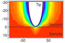
Schematic of AlGaN/GaN HEMT and its surface trapped charge (reliability issue) at off-state.
Research Tools
Simulation is a very flexible modelling approach in the area of GaN HEMTs where experimental techniques are not sufficient. We use commercial Silvaco simulation software with 30 interactive licenses.
Silvaco software provides unique capabilities including: (i) 2D/3D device modelling, (ii) drift-diffusion and hydrodynamic carrier transport modelling, (iii) surface defect analysis, (iv) bulk defect analysis, (v) transient simulation, (vi) thermal modelling, and (vii) wide-bandgap breakdown modelling.
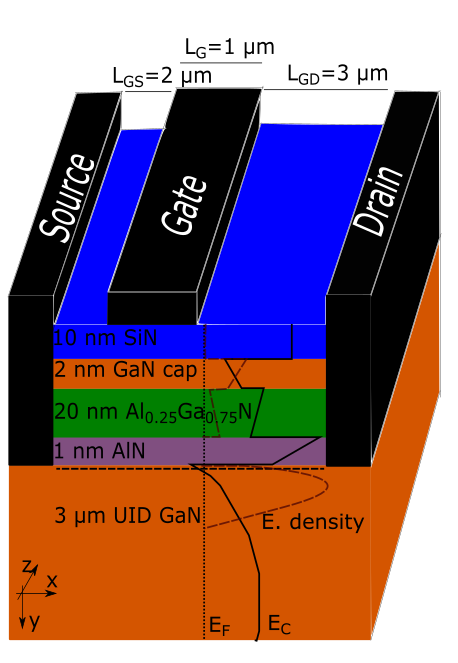
Simulated ID-VG characteristics at indicated VD's for the 1μm gate length GaN(cap)/Al0.25G0.75N/AlN/GaN HEMT compared to experimental data.
Parallel 3D finite element ensemble Monte Carlo device simulations
Parallel 3D finite element ensemble Monte Carlo device simulations have the following capabilities:
- 3D unstructured device mesh using tetrahedral elements
- Ensemble Monte Carlo engine with transport model for Si, strain Si, and III-V semiconductors
- Scattering mechanisms:
- Bulk related:
- polar optical phonons
- inter/intra-valley optical phonons
- acoustic phonons
- ionized and neutral impurities (screening models: Debye-Hückel, Thomas-Fermi, static, q-dependent)
- alloy scattering
- Dielectric-semiconductor interface related:
- interface roughness
- interface phonons
- Bulk related:
- Fermi-Dirac (self-consistent) or Boltzmann statistics
- quantum corrections using 1) a density gradient approach (adapted for the finite elements) or 2) a newly developed 2D finite element Schroedinger Equation solution
- finite element mesh adapted electric field calculations, charge assignment, contact treatment, and interface roughness/phonons
- atomistic dopants
2D finite element ensemble Monte Carlo device simulations
2D finite element ensemble Monte Carlo device simulations have the following capabilities:
- 2D device mesh using quadrilateral elements
- Ensemble Monte Carlo engine with transport model for Si, strain Si, and III-V semiconductors
- Scattering mechanisms:
Bulk related:
- polar optical phonons
- inter/intra-valley optical phonons
- acoustic phonons
- ionized and neutral impurities (screening models: Debye-Hückel, Thomas-Fermi, static, q-dependent)
- alloy scattering
Dielectric-semiconductor interface related:
- interface roughness
- interface phonons
- Fermi-Dirac (self-consistent) or Boltzmann statistics
- Quantum corrections using a effective quantum potential
- Finite element mesh adapted electric field calculations, charge assignment, contact treatment, and interface roughness/phonons
Quantum Transport: Parallel 2D Non-Equilibrium Green's Function (NEGF) simulations
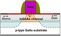
When the dimensions of semiconductor devices are on nanoscale, the carrier transport has to be described using quantum-mechanics. The quantum phenomena can be utilised to achieve unique properties and functionality of semiconductor devices at nanoscale. We are using quantum transport techniques to simulate nanoscale transistors in 2D real space like bulk/double gate Si MOSFET and Implant Free InGaAs MOSFET.
-simulations.jpg)
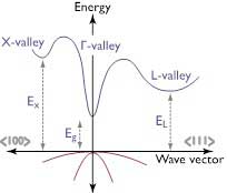
- uses a full 2D real space representation
- includes Γ and L valleys
- Simulated nanoscale transistors: bulk/double gate Si MOSFET and Implant Free InGaAs MOSFET
- Uses a full 2D real space representation
- Includes Γ and L valleys
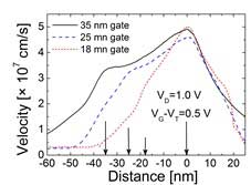
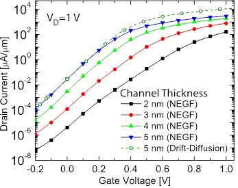
Study of the 20 nm gate length Implant Free In0.53Ga0.47As MOSFET:
ID-VG characteristics of the 20 nm gate length Implant Free In0.53Ga0.47As MOSFET for different channel thicknesses.
Band structure of InXGa1-XAs materials. The energy gap between the -L valleys is between 300 meV and 500 meV in dependence on the Indium content (x).
Conduction band and electron density profiles at the middle of the device (VG=0.9V) for the 5 nm channel thickness.
-for-the-5-nm-channel-thickness.jpg)
Quantum Transport: Parallel 3D Non-Equilibrium Green's Function (NEGF) simulations
When dimensions of semiconductor devices are on the nanoscale in all directions, 3D quantum transport has to be considered. We are using then 3D real-space Non-Equilibrium Green's Function technique to simulate the quantum transport in nanowire and Fin-like field effect transistors for future digital applications.
- simulated nanoscale transistors: Si FinFETs and nanowire transistors
- uses a mode space or a 3D real space representations.
- considering surface roughness
- including random discrete dopants
- in presence of electron-phonon scattering
- the effect of exchange-correlation has been taken into account in a Local Density Approximation (LDA).
- Simulated nanoscale transistors: Si FinFETs and nanowire transistors
- Uses a mode space or a 3D real space representations.
All simulations use the recursive algorithm for Gr and G<.
- considering surface roughness
- including random discrete dopants
- in presence of electron-phonon scattering
- the effect of exchange-correlation has been taken into account in a Local Density Approximation (LDA).
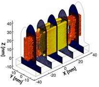
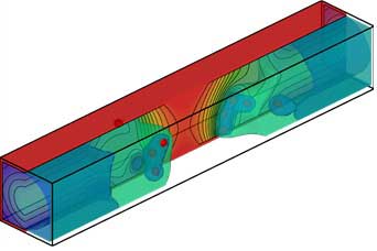
Study of silicon nanowire transistors:
![]()
Spectral density in silicon junctionless nanowire transistor showing the local potential of the impurities in the channel.
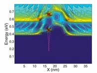
Current spectral density for nanowire with a dopant in the middle of the channel.
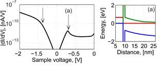
Modelling of scanning probe microscopy
R. J. Cobley, K. Kalna and Olga Krychenkova.
As the active regions of electronic materials and devices reduce in size to the nanoscale, the analysis tools need to characterise those with a spatial resolution in the same length scale. Scanning probe microscopy is one such technique and can be used to make surface electronic, morphological, optical, chemical and magnetic measurements down to the atomic scale. Unlike most electron microscopy techniques, scanning probe microscopy can be applied to biased devices under operation. The main limitation of the method is that with all scanning probe microscopy techniques the probe can interact electrostatically and physically with the sample, changing the measured properties of the device under test. We model scanning probe microscopy within TCAD Silvaco Atlas software using 2D finite element device simulations which have the following capabilities:
- self-consistent physically based modelling
- direct quantum tunnelling model using Price and Radcliffe formalism
- arbitrary realistic tip shapes
- full device transport models for scanning probe miscroscopy on devices
- realistic interaction of the probe and sample using a tip-induced band-bending
- image force correction can be included in the simulations
- modelling of the spectra obtained from scanning probe miscroscopy on powered devices
- including the effect of surface states